Information contained in this news release is current as of the date of the press announcement, but may be subject to change without prior notice.
HPSD and Hitachi Commercializes TED-MOS, a Newly Structured SiC Power Device That Balances Durability and Low Power Consumption Features (PDF Type, 283 kByte)
January 26, 2021
HPSD and Hitachi Commercializes TED-MOS, a Newly Structured SiC Power Device That Balances Durability and Low Power Consumption Features
Contributing to creating a decarbonized society by improving the efficiency and energy saving performance of devices responsible for power generation, transmission, transformation and electrification
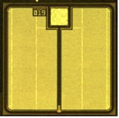
TED-MOS, a Newly Structured SiC Power Device
Tokyo, January 26, 2021 – Hitachi Power Semiconductor Device, Ltd. (“HPSD”) today announced that it will begin sample shipments of Trench Etched DMOS-FET (hereinafter referred to as “TED-MOS”), a fin-shaped trench (1) MOSFET (2) from March 2021. This is a new power device product (3) that uses silicon carbide (SiC), next-generation material that enables improved electrical efficiency to deliver power saving in various equipment and facilities that form key social infrastructure such as power systems, railway systems, electric vehicles and data centers.
TED-MOS is the commercialized version of the high durability-structured SiC power device developed by Hitachi, Ltd. (TSE: 6501, “Hitachi”) in August 2018 (4). One of core issues with conventional SiC power devices is that electrical fields concentrate around the base corners of the trench on the semiconductor chip surface, making it difficult to realize strong durability. TED-MOS overcomes this by forming fins in the trenches and employing a proprietary Hitachi structure that provides an electric current path on the side walls of the fins. In commercializing this product, HPSD and Hitachi employed a new development technique that enables short-circuit tolerance (5) and resistance to be optimized independently. This achieves a reduced cell pitch and optimized current path design with the lowest resistance to deliver the industry’s highest level of durability and low power consumption characteristics, whilst also providing a greater design freedom to enable the development of product designs tailored to a variety of uses. Through the provision of TED-MOS, HPSD will help reduce power consumption and carbon dioxide emissions for various social infrastructure facilities, contributing to the expansion of a decarbonized society.
With global energy demand expected to increase, power semiconductor devices are being utilized for a wide range of social infrastructure, and products demand ever higher efficiency and improved energy saving performance to enable the creation of a decarbonized society. Given these conditions, improving the performance of SiC power devices will offer benefits in industrial fields, including offshore wind power (listed as a key field in the Ministry of Economy, Trade and Industry’s “Green Growth Strategy Towards 2050 Carbon Neutrality”), next-generation solar, logistics and public transport such as rail, automotive, as well as storage batteries, telecommunications and marine vessels. These improvements will lead to energy savings in inverter and converter systems handling power generation, transmission, transformation and electrification by making them more efficient, smaller, lighter and by simplifying cooling mechanisms through high heat resistance.
To help create a decarbonized society, Hitachi and HPSD have developed and provided a range of power electronics products for rail and electric vehicles. In 2018, Hitachi announced the development of TED-MOS (now commercialized) as a SiC power device that further enhances the performance of the existing SiC DMOS-FET (6) product in terms of high current capacity, low power consumption and so on.
TED-MOS products seek to balance durability with power consumption, which has been an issue for SiC power device solutions. This is achieved by setting up a “field relaxation layer” to significantly reduce electric field intensity and a “current spreading layer” to lower resistance around the center of the device, and by adopting a device structure that uses the walls of the fin-shaped trenches made from a low-resistance crystal surface as the electric current path. In addition, by applying a new development technique allowing short-circuit tolerance and resistance to be optimized independently, enabling a reduced cell pitch and optimized current path design with the lowest resistance. Compared with initial the prototype developed in 2018, short-circuit tolerance has been improved 20% whilst resistance has been lowered 40% while maintaining the 1.2kV withstand voltage required for commercialization.
Moving forward, in addition to the product lines for transportation equipment developed and provided to date, Hitachi and HPSD will work to develop and provide products aimed at innovation in social infrastructure to contribute to creating a decarbonized society.
——-
- (1)A structure that creates an electric current path using the side walls of fins formed by digging trenches.
- (2) MOSFET: Metal-Oxide-Semiconductor Field-Effect-Transistor
- (3) A semiconductor device used in power conversion such as inverters and converters that controls electric currents through switching.
- (4) Hitachi press release: “Highly durable silicon carbide (SiC) power semiconductor TED-MOS for energy saving in electric vehicle motors” (August 30, 2018)
- (5) The time until a power device breaks during short circuit
- (6) DMOS-FET: Double Diffused MOSFET
The development technique for TED-MOS, balancing durability with low power consumption
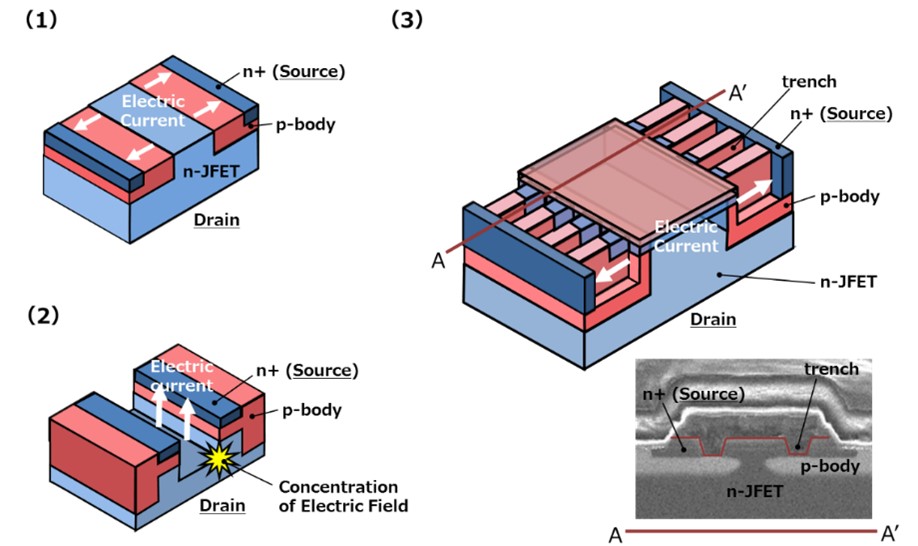
SiC power devices have a performance advantage over their conventional silicon (Si) counterparts due to their high-speed switch on and switch off performance as they conduct electricity more easily. While this makes them well suited for reducing the power consumption of power converters, unlike Silicon, the ease of electricity transmission (resistance) varies depending on the crystal plane. For this reason, whilst trench SiC MOSFET [(2) in Figure 1] devices that conduct current on a lower-resistance crystal plane than conventional DMOS-FET [(1) in Figure 1)] devices, have been commercialized, these structures are prone to the electric field concentration at the bottom corners of the trenches, making it difficult to achieve a balance between low resistance and reliable durability. Additionally, as durability and resistance are determined based on a single trench structure, designing devices to suit a wide range of fields may pose a challenge.
To address this and achieve both durability and low power consumption, with TED-MOS a “field relaxation layer” was placed on the center of the device to mitigate how voltage is applied and significantly reduce the intensity of the electric field. A “current spreading layer” was positioned to lower resistance at the center of the device, which provides an electric current path connecting to the side walls of the fin-shaped trenches made from a low-resistance crystal surface even within the SiC [(3) in Figure 1]. In the latest iteration, by enabling a design that independently optimizes the n-JFET component in the center of the device for short-circuit tolerance (an indicator of durability) and the trench part for resistance (an indicator of power consumption), the issue of device design freedom was resolved. A cell pitch reduction and optimization of electric current flow, with a low electrical resistance, further enhanced durability and low power consumption.
By using these features as core technologies to shorten device development times, HPSD and Hitachi will help a growing base of customers in the environmental business expand their power electronics products.

Figure 1: SiC power device structure
TED-MOS Specifications
| Product Series | Voltage | Current | Schedule for Start of Sample Shipments |
|---|---|---|---|
| SiC TED-MOS | 1.2kV | 35 A~ | March 2021 |
HPSD’s Contributions to Energy Savings
To help create a decarbonized society, HPSD has released various power electronics products such as the HiGT (7) series with 1.7-6.5kV withstand voltage for the rail industry and the 6-in-1 direct water-cooled IGBT (8) series for electric vehicles. In 2016, Hitachi released the SiC DMOS-FET product for the railway industry that was compact but enabled control at the world’s highest current levels. This helped reduce the size and weight of vehicle components, while its low loss characteristics helped reduce power consumption by around 30% compared with vehicles employing the conventional IGBT technology. TED-MOS employs next-generation technologies that further enhance the features of SiC DMOS-FET such as high current capacity and low power loss and is expected to contribute to further reductions in power consumption.
- (7) HiGT:High-Conductivity IGBT
- (8) IGBT:Insulated Gate Bipolar Transistor
Note
TED-MOS is a registered trademark of Hitachi, Ltd. in Japan, the U.S., the U.K., South Korea, China, Taiwan and EUIPO.
About Hitachi Ltd.
Hitachi, Ltd. (TSE: 6501), headquartered in Tokyo, Japan, is focused on its Social Innovation Business that combines information technology (IT), operational technology (OT) and products. The company’s consolidated revenues for fiscal year 2019 (ended March 31, 2020) totaled 8,767.2 billion yen ($80.4 billion), and it employed approximately 301,000 people worldwide. Hitachi drives digital innovation across five sectors – Mobility, Smart Life, Industry, Energy and IT – through Lumada, Hitachi’s advanced digital solutions, services, and technologies for turning data into insights to drive digital innovation. Its purpose is to deliver solutions that increase social, environmental and economic value for its customers. For more information on Hitachi, please visit the company’s website at www.hitachi.com.
Contact:
Hitachi Power Semiconductor Device, Ltd.
Inquiry Form


